WSU_tools
Substrate Preparation
Clean hood, fume hood, and vacuum oven facilities enable safe and particle-free environments for substrate cleaving, cleaning, wet chemistry, and surface treatments for electronic-grade device substrates.
Solution Deposition
A dedicated glovebox facility creates a pristine nitrogen environment for solution deposition of optoelectronic thin films. The atmosphere is actively scrubbed to <0.1ppm of O2 and ~0.1ppm of H2O as well as activated carbon solvent removal from the atmosphere. Inside a microbalance is used to precisely weigh materials for solution prep. A spincoater casts standard thin films, while a custom blade coater mimics roll-to-roll deposition and additionally is capable of in-situ UV-visible spectroscopy to monitor the film formation process.
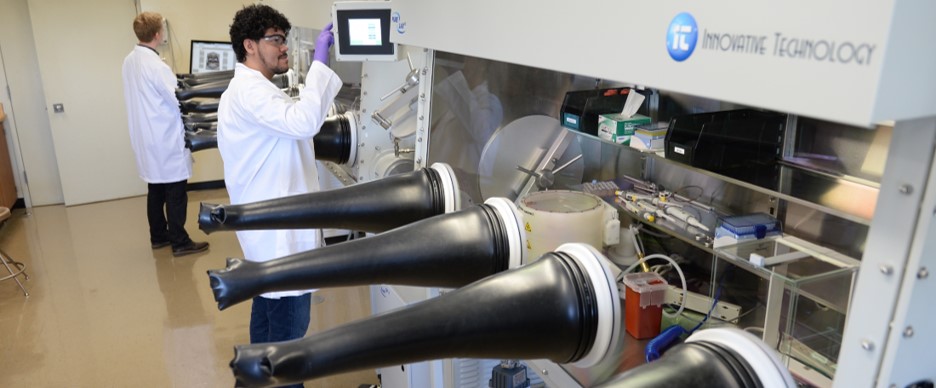
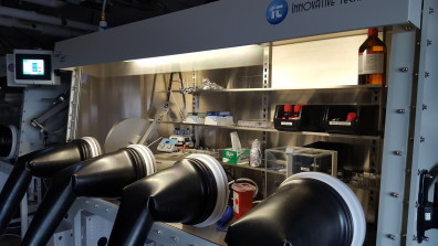
 Physical Vapor Deposition
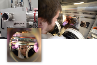
The Angstrom Engineering NexDep is fully computer automated for multilayer-multisource thin film physical vapor deposition. The instrument is coupled into the glovebox to eliminate exposure to the atmosphere for pumpdown to <1×10^-7 Torr base pressure in <20 minutes. This enables high-throughput depositions (many per day versus a single high vacuum deposition per day). Six sources include four thermal sources with one source water-cooled, enabling >2000C deposition temperatures (e.g. SiOx or Titanium). Two additional temperature-controlled RADAK sources specialize in depositing molecular materials to avoid degradation. Multiple quartz crystal monitors not only enable controlled thickness and deposition rate, but also control of individual components and composition during codeposition of composite films. The substrate temperature can also be actively controlled from -150C to 400C enabling control of molecular dynamics during deposition as well as post annealing treatments. Full computer control enables programed, reproducible sample recipes.
Device Test Bed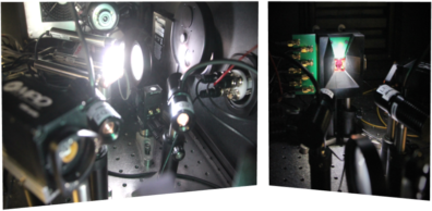
A custom light-controlled and temperature-stabilized device probe station within a dedicated glovebox enables pristine, state-of-the-art testing and measurement of optoelectronic devices. Four 2-terminal devices are individually probed with a 2-GHz bandwidth switch and high-throughput pogo-pin contacts for no-tool chip switching. An articulated computer-controlled mirror enables beam-steering optimization on devices for light coupled from behind the glovebox. High-power LEDs enable DC light-biasing while an avalanche photodiode is used for time-resolved photoluminescence (trPL).
Light Sources and Light Management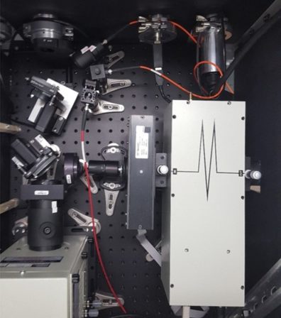
Our repertoire of light sources include an AAA AM1.5G solar simulated spectrum, a chopped monochromated light spectrum (e.g. photocurrent spectroscopy), a nanosecond pulsed wavelength-tunable laser (for time-delayed collection field ‘TDCF’ or transient photovolatage ‘TPV’), and monochromatic picosecond 80MHz pulsed laser (trPL).
All light sources are computer-controlled and selected. They are all coupled into the glovebox onto the same device testbed, making possible a preprogramed suite of optoelectronic measurements with high reproducibility and throughput.
Electronics Measurement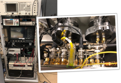
Each device on a chip is measured via an automated sequence with specific measurements and test parameters coded by the researcher. A 2 GHz switch enables automated electrical connections to up to eight devices on a substrate while conducting nanosecond pulsed electronics at 50 Ohm equivalent impedance. The Keithley 2450 enables DC IV measurements (e.g. power curves for solar cells or luminescence effficiency for OLEDs). The LeCroy GHz 12-bit dynamic range oscilloscope is paired with the 240 MHz Tektronix function generator and custom amplifiers for measurement of nanosecond device dynamics (e.g. TDCF, TPV). A Princeton lock-in amplifier enables high sensitivity spectroscopy. A PicoQuant timer is used for trPL .
Spectroscopy
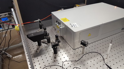
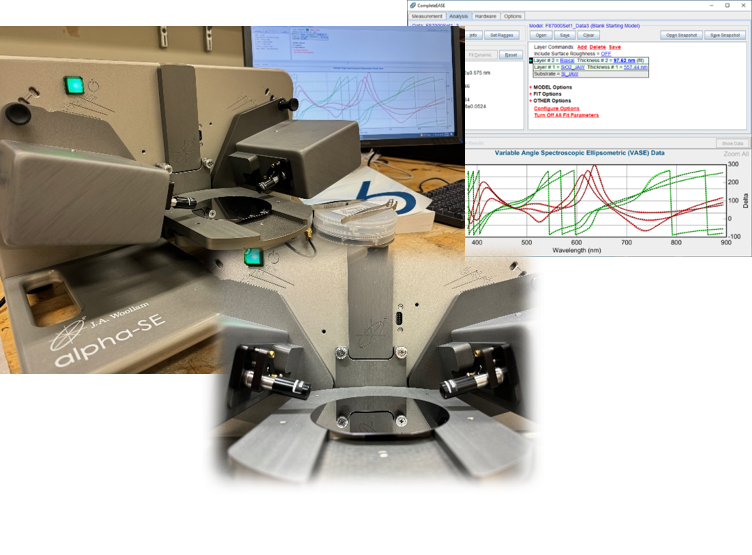
We are able to complete advanced configuration absorption, photoluminescence, and electroluminescence spectroscopy across the UV-visible-NIR range (wavelengths 300-1700nm). Using fiber-coupled motorless high-efficiency spectrometers, we acquire spectra at high speed (10ms), in-situ to printing deposition, or during device operation. The Washington State JCDREAM program has funded the Woolam Alpha-SE Variable Angle Spectroscopic Ellipsometer (VASE). VASE enables non-destructive multilayer film thickness measurement as well as quantitative spectral characterization of material complex/tensor index of refraction.
Microscopy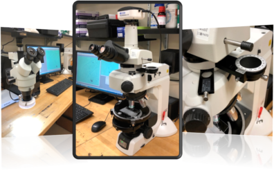
A Nikon Eclipse LV100 polarzied optical microscope is used for micrographs of birefringent or dichroic micro domains in organic films. A binoscope enables convenient magnified viewing of small samples. Both scopes are CCD-coupled for full image documentation.